SmartDB compact redesign — board routing complete
Updated 2026-10-10. Fully routed bench prototype; fabrication review remains.
Open smart_db.kicad_pro in KiCad. The editable
schematic, PCB, project-local symbol and
footprint libraries are saved together here. This is the permanent v2 project,
moved from ../compact_wip/. The previous routed bench revision and its reports
are preserved in the archive.
Saved work
Draft 95 × 78 mm four-layer placement, outward-facing connectors and four M3 mounting holes with screw-head copper clearances.
Revised AP63203 buck supply, bulk/local decoupling, ADC supply filter and test points.
Schematic organized into six numbered subsystem boxes.
Monochrome vector logo extracted from the cover of
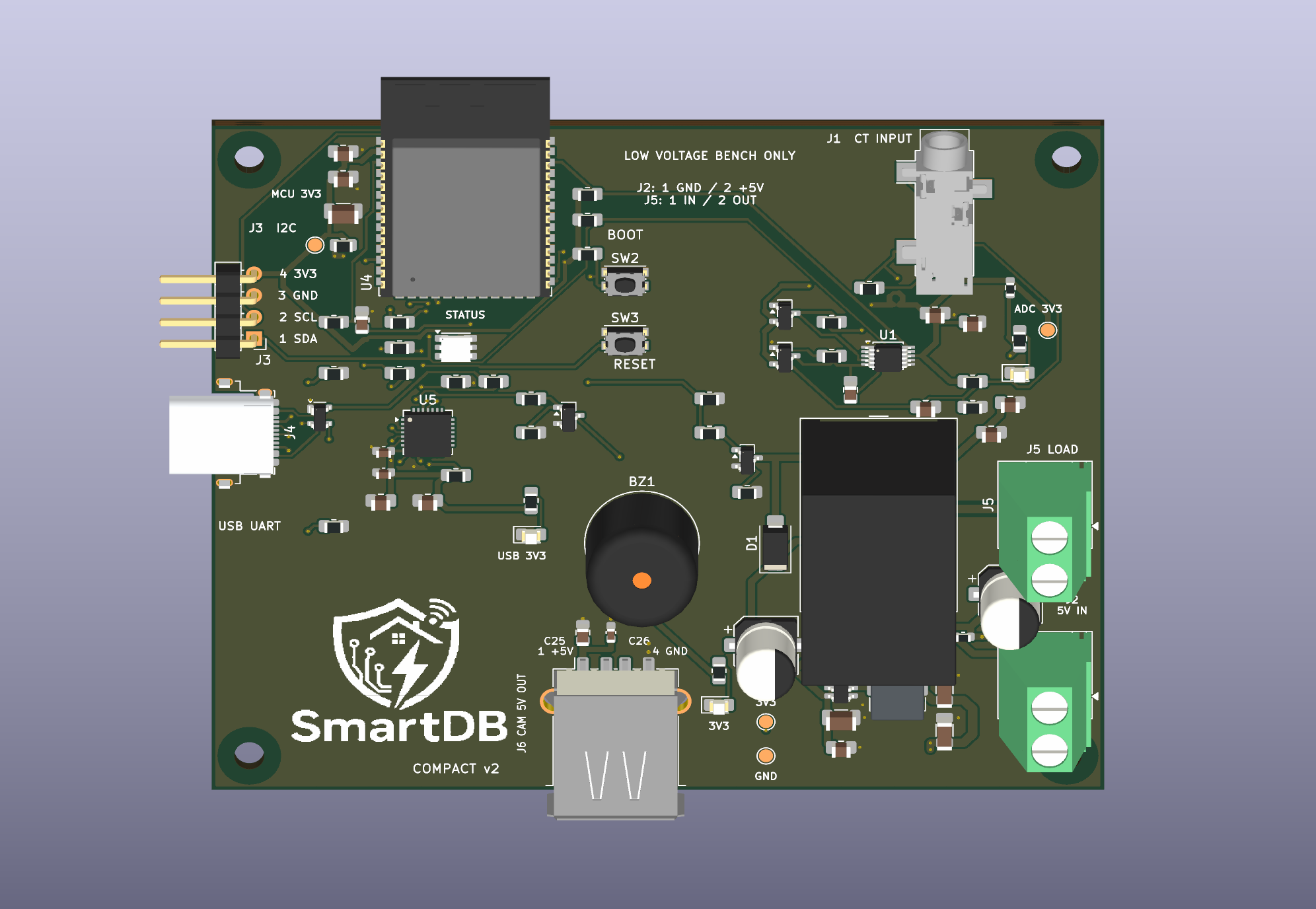
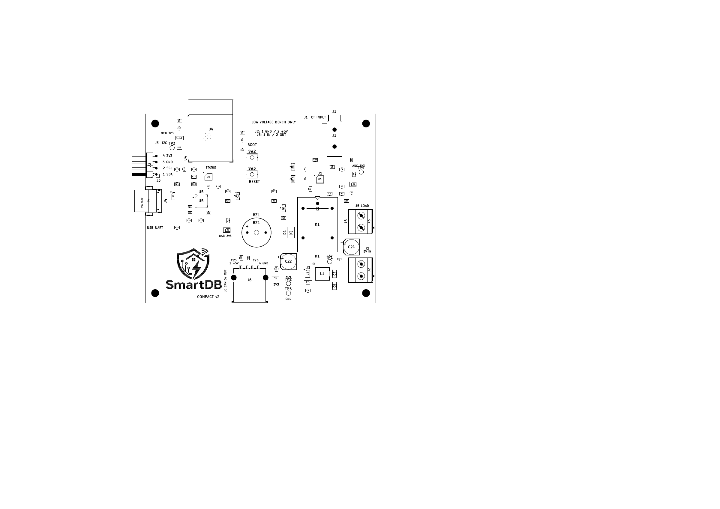
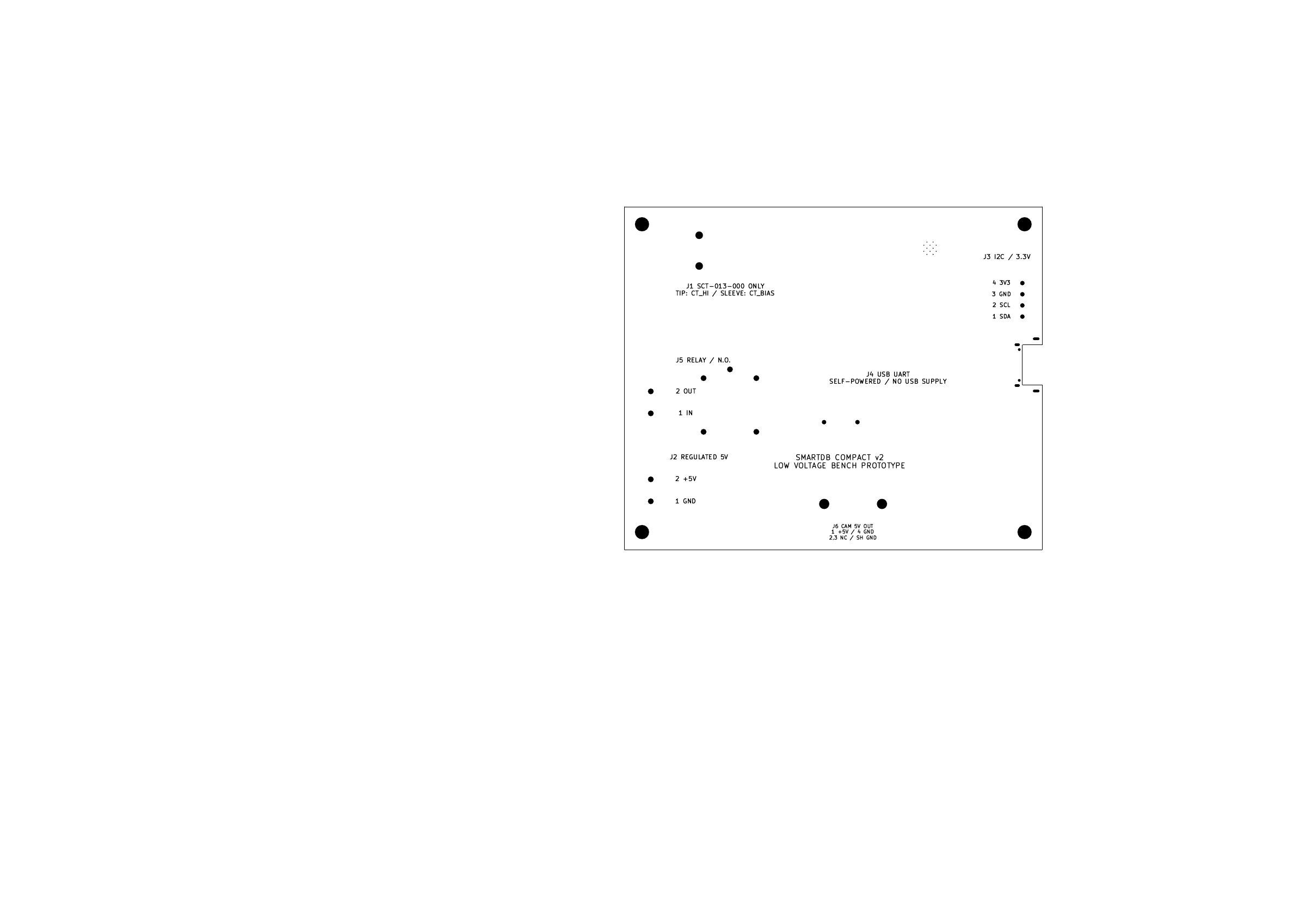
formal_docs/proposal/SmartDB_proposal_final.pdf, saved as work/smartdb-logo-monochrome.svg. The logo is now on the front silkscreen, together with functional connector, BOOT/RESET, status and power labels. The back has connector pin and polarity labels.Corrected overlaps involving the relay flyback diode, MCU reset capacitor/pullup, ADC decoupling and relay-coil decoupling. The local ESP32 footprint now matches the board, including its four-layer antenna keepout and edge silkscreen treatment.

Connector access and routing
Working board construction: four-layer FR-4, 1.6 mm overall thickness, 1 oz outer copper and 0.5 oz inner copper, following the request for standard construction. The layer order is signal/power–ground–ground–signal/power. Manufacturer-specific dielectric spacing remains to be selected.
J3 is the four-pin I²C header. Its pins now project approximately 5.5 mm past the left board edge. Front and back labels identify 1 SDA, 2 SCL, 3 GND, 4 3V3. J2 remains the two-pin regulated 5 V screw terminal.
J4 moved 7.64 mm toward the left edge. Its original mid-mount cutout is retained; the unnecessary additional recess is removed. D7 moved 6 mm toward the connector.
All nets are routed, including buck supply, relay/load, ADC, I²C, UART, USB, reset/boot, LEDs and buzzer. Signals remain on F.Cu and B.Cu; both inner layers remain ground planes. Final copper contains 608 segments and 88 vias.
The buck switch and bootstrap connections are short front-layer routes. The output has a wider distribution path and separate feedback branch. Load contacts use 1 mm traces without vias. Ground stitches connect the ADC, input protection, decoupling and MCU regions to the inner planes.
R13 moved to (73, 70) mm to open a clean reset/enable routing path.
The USB main pair is manually routed, with 0.2 mm traces, 0.3 mm gap and two layer transitions per main path. Preferred widths are now 0.30 mm for signals, 0.60 mm for power, 0.75 mm for the 5 V/coil supply and 1.00 mm for load contacts. Actual routing retains narrower sections in congested channels and pad escapes; the minimum is 0.20 mm. USB dimensions were preserved.
USB appearance now uses a simplified local visualization, clearly identified in
SmartDB.3dshapes/. The manufacturer STEP download returned HTTP 403, and KiCad’s referenced model was unavailable. This is not an enclosure-fit model.
STEP export
smart_db.step now exports successfully with all three previously
problematic parts included. D6, J1 and J4 reference project-local STEP files through
${KIPRJMOD}. J1 uses the official Same Sky model,
aligned to the footprint. D6 uses a simplified 3.5 × 2.8 × 0.6 mm package preview
based on ROHM’s drawing, page 263.
J4 uses a STEP solid version of the existing simplified USB preview. D6 and J4
are visual approximations, not certified enclosure-fit models.
Model sources and transforms are recorded in SmartDB.3dshapes/provenance.json.
The model fix preserves all copper, pads, placements and rules. Its original CAD
and incomplete STEP are preserved in work/before_step_model_fix/.
Reopen the PCB from disk before exporting in an already-open KiCad window;
an old editor buffer still contains the previous model references.
Two-camera connections
J3: MLX90640 thermal camera, 1 SDA / 2 SCL / 3 GND / 4 3V3.
J6: USB-A 5 V camera power output, using a TE 292303-7 socket with SMD contacts and two through-hole shell anchors. Connect a short USB-A to micro-USB cable to the external ESP32-CAM-MB base shown in the reference photo. USB pin 1 is +5V, pin 4 and the shell are ground; pins 2 and 3 are intentionally unconnected. This is a dedicated camera power connection, with no USB host, data, programming or charging-port negotiation on J6.
J6 is at the bottom edge, at (103, 117.3) mm. It branches from F1’s protected output, with a 1.0 mm main trace on B.Cu, a 0.75 mm fuse-pad connection and paired 0.8/0.4 mm vias at both ends. A 0.75 mm front-layer connection reaches VBUS without crossing the existing 3.3 V route. C25 (10 µF, 16 V, X7R, 0805) and C26 (100 nF, 16 V, X7R, 0603) provide local bypassing near J6; capacitor and connector ground vias join the internal planes. All pre-camera routes and placements are preserved. The logo was reduced and moved left for clearance. The local USB-A footprint only moves the three edge-clipped silkscreen segments to F.Fab; contact pads and the KiCad STEP model are unchanged. TE recommends 1.42 mm PCB thickness for this connector; verify shell retention and soldering with actual parts on the project’s 1.6 mm PCB before fabrication release. F1’s symbol now correctly identifies its specified part as a one-time fast-acting fuse, rather than a resettable device.
Wi-Fi is the image-data path. The current PlatformIO ESP-IDF firmware
has an esp32cam target serving authenticated fresh QVGA JPEGs at /capture, and a
smartdb_s3 target combining those images with MLX90640 data. This is request-driven
capture, not a USB video stream. Real alignment and capture timing still need hardware validation.
The older SD-card diagnostic camera project remains separate.
Run the firmware project’s ./setup.sh menu or its SmartDB: Setup VS Code task to
install/configure each board. Program the camera by connecting its base directly to the
computer; J6 cannot program it. Configure the camera first so the menu can supply its Wi-Fi
address to the S3. Subsequent Wi-Fi/token/endpoint changes persist in NVS without reflashing;
protection limits are also configurable through the menu, with physical re-arm still required.
Supply both boards through J2 from regulated 5 V; a 2 A capable source is a
provisional supply target. J4 USB-C remains the data/programming connection;
J6 USB-A supplies camera power. The shared 1.5 A F1 is not
an independent camera current limiter. Reserve 0.5 A for the camera/base and target
no more than 1.1 A combined continuous input at 25°C; this is a design budget,
not a measured current rating. Temperature derating, simultaneous Wi-Fi bursts,
camera flash/SD activity, startup and cable voltage drop still need validation.
See power review and sources. The pre-addition
CAD and reports are preserved in work/before_camera_power/; the preceding
JST camera-power revision is preserved in work/before_camera_usb/.
See routing review, copper PDF and 3D preview. Existing placement, schematic and label previews below have also been regenerated.
Validation status and remaining work
Current KiCad 10.0.6 results: ERC 0 violations; PCB DRC 0 geometric/library/silkscreen violations, 0 unconnected items, 0 schematic/PCB mismatches. No clearance rules, DRC severities or exclusions were changed. Default and Power preferred widths changed to 0.30 and 0.60 mm at the user’s request. The resume baseline had 22 placement violations (including three pad shorts), 113 unconnected items and no parity issues.
Current review outputs:
Schematic PDF and netlist
ERC, DRC, and source hashes and checks
Files without the current suffix remain historical intermediate outputs.
work/resume_backup/ preserves the board, schematic, project and local footprint
as they were at the start of this continuation. SNAPSHOT.json describes the
original paused snapshot; it is not the hash manifest for today’s revised sources.
Routing is complete. USB impedance and timing still need manufacturer stackup review and measurement. The selected 1 oz construction does not qualify the buck circuit for its IC’s maximum 2 A rating; current and thermal limits require review. Check connector access, mounting clearances, capacitor placement, current paths, voltage drop, USB geometry, antenna clearance and silkscreen. Recheck labels after routing and regenerate the review outputs. Verify the exact supply, component selections and capacitor derating before fabrication. Hardware load-step, brownout, relay, thermal, USB and ADC-noise measurements remain necessary; a rule-check pass cannot establish that assembled hardware works.
No enclosure dimensions or J2 supply model have been confirmed. The design remains scoped to a regulated 5 V supply and a provisional 5–24 V DC, up-to-1 A resistive relay test load. No mains use.
Resuming the editing scripts
work/ preserves the staging scripts and evidence; work/helpers/ preserves
helpers they import. They contain original absolute /tmp/smartdb_review/...
paths and some rebuild earlier stages. Do not run them blindly against this
snapshot. Restore the original staging structure or review/update paths first.
The files at this snapshot’s root are the authoritative saved CAD state.
SNAPSHOT.json records the original paths and hashes of all copied files.
The new work/resume_placement.py and work/add_board_labels.py resolve paths
relative to this project. The first requires KiCad’s Python runtime and refuses
to move components once tracks/vias exist; the second uses ordinary Python and
replaces only its own deterministically identified graphics. In this environment:
flatpak run --command=python3 org.kicad.KiCad work/resume_placement.py
python3 work/add_board_labels.py
These are placement-stage tools. Do not replay placement after hand edits without
reviewing its explicit coordinates. Use work/validate_current.py after generating
fresh ERC, DRC and netlist outputs to refresh the source-hash/check manifest.
The connector/routing scripts added in this session are preserved as engineering
work records, not a one-command rebuild pipeline. Some restore earlier board
stages or append copper. Do not replay them on the current routed board.
The root CAD files and work/validation_current.json are authoritative. The
older drc_placement_current.json describes the placement-only milestone.
work/routed_checkpoint/ preserves the completed CAD and final DRC report.
work/full_routing_backup/ preserves the earlier partially routed state.
An older editor copy saved during routing is preserved separately in
work/editor_saved_during_routing.kicad_pcb. Reopen the project before editing
so an old editor buffer does not overwrite the completed routes.